

Intel’s next-generation Meteor Lake laptop processors are nearing release—the company announced this week that the first processors will launch on December 14. It’s unclear whether actual Core and Core Ultra systems will be available to buy on that date, but at a bare minimum, the official announcement will pave the way to many laptop announcements at CES in January.
We already know a lot of basic facts about Meteor Lake; it uses a combination of chiplets manufactured by both Intel and TSMC rather than a single monolithic die, and it will mark the retirement of Intel’s “nth-generation” and i3/i5/i7/i9 branding. We also know that it won’t be ready for desktops and that the next round of Core desktop CPUs will be very similar to the 12th- and 13th-generation chips.
But at Intel’s Innovation event this week, the company dove a little deeper into some of Meteor Lake’s advancements, describing more about how the chips would balance E-cores and P-cores and announcing its most substantial integrated GPU upgrade in years. We’ll hit some highlights below, though it’s worth watching or reading the full presentation to find out more.
Tiles for miles

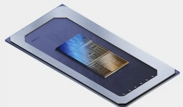
Meteor Lake will be Intel’s first consumer processor to move to a chiplet-based design—instead of being one monolithic die that contains the CPU, GPU, and all the other bits and pieces needed for a modern laptop CPU, Meteor Lake is split into four “tiles”that are joined together by a fifth base tile that allows them to communicate with each other. The process of stacking the chiplets on top of the base tile is a packaging technology that Intel calls Foveros.
Here’s a basic breakdown of what is in each of those four tiles:
- The compute tile is where most of the actual CPU is. Intel’s current renderings show a chip with six high-performance P-cores based on the Redwood Cove architecture, and eight high-efficiency E-cores based on the Crestmont architecture.
- The graphics tile is where most graphics processing happens, though a few specific functions that you’d usually find in a GPU have been moved to other tiles. Meteor Lake’s integrated GPU is mostly just an integrated version of an Intel Arc dedicated GPU, complete with hardware ray-tracing acceleration.
- The IO tile handles most external connectivity, including PCI Express 5.0 lanes and Thunderbolt 4 support (Thunderbolt 5 will need to wait).
- The SoC tile is probably the most interesting of the four. It includes two additional Crestmont E-cores, the media encoding and decoding engine that would normally be located in the GPU, and the neural processing unit (NPU) used for accelerating AI and machine learning workloads. It also handles Wi-Fi and Bluetooth connectivity and connecting to external displays over HDMI 2.1 and DisplayPort 2.1.
One of the notable things about Meteor Lake is that not all of the tiles are being manufactured by Intel. The compute tile, which houses the actual P-cores and most of the E-cores, uses the new Intel 4 process, an upgrade from the Intel 7 process used for most current Core chips. But the graphics tile is being made on a 5 nm TSMC process, while the IO tile and SoC tile are made on a 6 nm TSMC process.
Intel has also used TSMC’s manufacturing to make its Arc GPUs, so it’s not the first time we’ve seen these two chipmaking frenemies work together. But Intel is trying to catch up with TSMC’s manufacturing, and Intel sees its foundry operations as key to its future growth. I wouldn’t be surprised if moving back to all-Intel-made tiles is the eventual goal.
E-ven more E-cores

Intel has said that Meteor Lake’s P-cores don’t change much compared to the ones used in 12th- and 13th-generation Alder Lake and Raptor Lake CPUs—we may see higher clock speeds, but not much has changed in terms of instructions-per-clock or instruction set. The E-cores do get some improvements, though.
Meteor Lake actually includes two different kinds of E-cores. There are two low-power (LP) E-cores in the SoC tile, and the updated version of Intel’s Thread Director will attempt to use those E-cores for as many tasks as possible. Intel calls this chunk of the SoC tile the “low-power island”because the idea is to allow the compute tile and the graphics tile to completely power down as much as possible to save power.
When tasks require more performance than the LP E-cores can provide, Thread Director will kick them to the compute tile—either to the main E-core clusters, which are tuned to handle low-impact multithreaded workloads, or to the P-cores, which are used for single-threaded tasks and any multithreaded work the E-cores can’t handle. This is a change from how Thread Director works in 12th- and 13th-generation processors, where high-priority tasks would head straight to the P-cores without trying the E-cores first. (Though it remains to be seen whether the Thread Director changes will result in any kind of user-noticeable delays for high-performance tasks.)

Also worth noting: Crestmont E-cores can be added to processors in groups of two, where previous-generation Gracement E-cores could only be added in groups of four. This might make it easier for Intel to justify bringing small groups of E-cores to lower-end processors that didn’t have them before. All E-cores remain single-threaded, while P-cores still support two threads per core.
The new E-cores also include a few other niceties—VNNI instructions for accelerating AI workloads, and even AVX10, which brings many of the benefits of Intel’s AVX-512 instructions without requiring 512-bit registers. The 12th- and 13th-generation Core processors totally shut off AVX-512 support because the E-cores didn’t support it, even though support was present in the P-cores. This has created an awkward situation where AMD’s latest Zen 4 chips support the AVX-512 instructions that Intel invented and promoted, where Intel’s latest consumer chips don’t.